- 您现在的位置:买卖IC网 > Sheet目录2003 > LTC1279CG#TRPBF (Linear Technology)IC A/DCONV SAMPLNG W/SHTDN24SSOP
7
LTC1279
PI FU CTIO S
UU
U
AIN (Pin 1): Analog Input. 0V to 5V (Unipolar), ±2.5V
(Bipolar).
VREF (Pin 2): 2.42V Reference Output. Bypass to AGND
(10
F tantalum in parallel with 0.1F ceramic).
AGND (Pin 3): Analog Ground.
D11 to D4 (Pins 11 to 4): Three-State Data Outputs.
D11 is the Most Significant Bit.
DGND (Pin 12): Digital Ground.
D3 to D0 (Pins 13 to 16): Three-State Data Outputs.
DVDD (Pin17): Digital Power Supply, 5V. Tie to AVDD pin.
SHDN (Pin 18): Power Shutdown. The LTC1279 pow-
ers down when SHDN is low.
CONVST (Pin 19): Conversion Start Input. It is active
low. The falling edge of the CONVST signal initiates a
conversion. The LTC1279 responds to CONVST signal
only if the signal applied to CS is a logic low.
RD (Pin 20): READ Input. A logic low signal applied to
this pin enables the output data drivers when the signal
applied to the CS pin is a logic low.
CS (Pin 21): The CHIP SELECT input must be a logic low
for the ADC to recognize the signals applied to the
CONVST and RD inputs.
BUSY (Pin 22): The BUSY output shows the converter
status. It is a logic low during a conversion.
VSS (Pin 23): Negative Supply. – 5V will select bipolar
operation. Bypass to AGND with 0.1
F ceramic. Tie to
analog ground to select unipolar operation.
AVDD (Pin 24): Positive Supply, 5V. Bypass to AGND
(10
F tantalum in parallel with 0.1F ceramic).
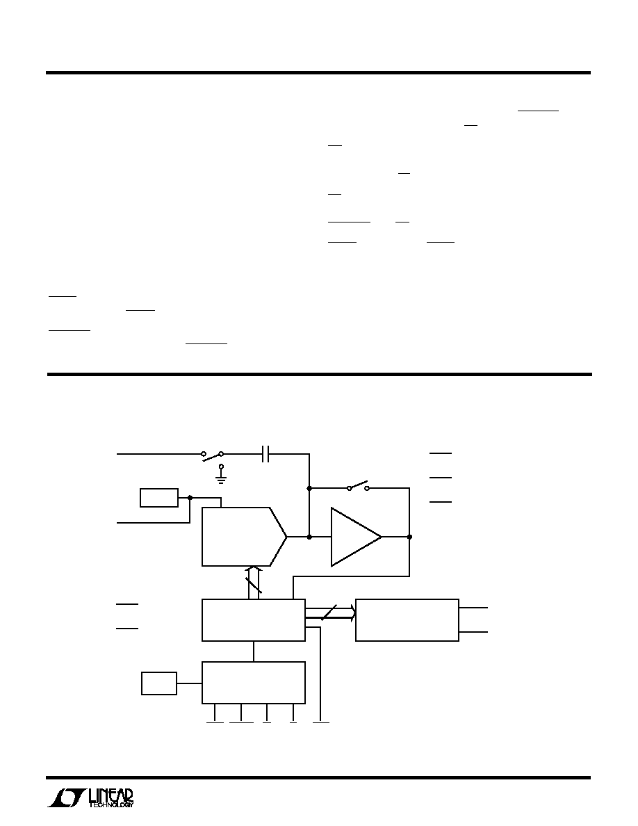
FU CTIO AL BLOCK DIAGRA
UU
W
12-BIT CAPACITIVE DAC
COMPAR-
ATOR
2.42V REF
VREF
CSAMPLE
SUCCESSIVE APPROXIMATION
REGISTER
OUTPUT LATCHES
D11
D0
BUSY
CONTROL LOGIC
CS
CONVST
RD
SHDN
INTERNAL
CLOCK
ZEROING
SWITCH
DVDD
VSS
AVDD
(0V FOR UNIPOLAR MODE
OR –5V FOR BIPOLAR MODE)
AIN
AGND
DGND
12
1279 BD
发布紧急采购,3分钟左右您将得到回复。
相关PDF资料
LTC1282ACN#PBF
IC A/D CONV SAMPLING W/REF 24DIP
LTC1288IS8#TRPBF
IC A/D CONV SAMPLING 12BIT 8SOIC
LTC1298IS8#TRPBF
IC A/D CONV SAMPLING 12BIT 8SOIC
LTC1327CNW#PBF
IC TXRX EIA/TIA-562 3.3V 28-DIP
LTC1329ACS8-50#TRPBF
IC D/A CONV 8BIT MICROPWR 8-SOIC
LTC1337CNW#PBF
IC 3DVR/5RCVR 5V RS232 28-DIP
LTC1382IN#PBF
IC TXRX 5V RS232 W/SHTDWN 18-DIP
LTC1383IS#TRPBF
IC TXRX 5V RS232 LOW PWR 16-SOIC
相关代理商/技术参数
LTC1279CSW
功能描述:IC A/DCONV SAMPLNG W/SHTDN24SOIC RoHS:否 类别:集成电路 (IC) >> 数据采集 - 模数转换器 系列:- 标准包装:1,000 系列:- 位数:12 采样率(每秒):300k 数据接口:并联 转换器数目:1 功率耗散(最大):75mW 电压电源:单电源 工作温度:0°C ~ 70°C 安装类型:表面贴装 封装/外壳:24-SOIC(0.295",7.50mm 宽) 供应商设备封装:24-SOIC 包装:带卷 (TR) 输入数目和类型:1 个单端,单极;1 个单端,双极
LTC1279CSW#PBF
功能描述:IC A/DCONV SAMPLNG W/SHTDN24SOIC RoHS:是 类别:集成电路 (IC) >> 数据采集 - 模数转换器 系列:- 其它有关文件:TSA1204 View All Specifications 标准包装:1 系列:- 位数:12 采样率(每秒):20M 数据接口:并联 转换器数目:2 功率耗散(最大):155mW 电压电源:模拟和数字 工作温度:-40°C ~ 85°C 安装类型:表面贴装 封装/外壳:48-TQFP 供应商设备封装:48-TQFP(7x7) 包装:Digi-Reel® 输入数目和类型:4 个单端,单极;2 个差分,单极 产品目录页面:1156 (CN2011-ZH PDF) 其它名称:497-5435-6
LTC1279CSW#TR
功能描述:IC ADC 12BIT SAMPL SHTDWN 24SOIC RoHS:否 类别:集成电路 (IC) >> 数据采集 - 模数转换器 系列:- 标准包装:1,000 系列:- 位数:12 采样率(每秒):300k 数据接口:并联 转换器数目:1 功率耗散(最大):75mW 电压电源:单电源 工作温度:0°C ~ 70°C 安装类型:表面贴装 封装/外壳:24-SOIC(0.295",7.50mm 宽) 供应商设备封装:24-SOIC 包装:带卷 (TR) 输入数目和类型:1 个单端,单极;1 个单端,双极
LTC1279CSW#TRPBF
功能描述:IC A/DCONV SAMPLNG W/SHTDN24SOIC RoHS:是 类别:集成电路 (IC) >> 数据采集 - 模数转换器 系列:- 标准包装:1,000 系列:- 位数:12 采样率(每秒):300k 数据接口:并联 转换器数目:1 功率耗散(最大):75mW 电压电源:单电源 工作温度:0°C ~ 70°C 安装类型:表面贴装 封装/外壳:24-SOIC(0.295",7.50mm 宽) 供应商设备封装:24-SOIC 包装:带卷 (TR) 输入数目和类型:1 个单端,单极;1 个单端,双极
LTC1279CSWPBF
制造商:Linear Technology 功能描述:LTC1279CSWPBF
LTC1279IG
功能描述:IC A/DCONV SAMPLNG W/SHTDN24SSOP RoHS:否 类别:集成电路 (IC) >> 数据采集 - 模数转换器 系列:- 标准包装:1,000 系列:- 位数:12 采样率(每秒):300k 数据接口:并联 转换器数目:1 功率耗散(最大):75mW 电压电源:单电源 工作温度:0°C ~ 70°C 安装类型:表面贴装 封装/外壳:24-SOIC(0.295",7.50mm 宽) 供应商设备封装:24-SOIC 包装:带卷 (TR) 输入数目和类型:1 个单端,单极;1 个单端,双极
LTC1279IG#PBF
功能描述:IC A/DCONV SAMPLNG W/SHTDN24SSOP RoHS:是 类别:集成电路 (IC) >> 数据采集 - 模数转换器 系列:- 标准包装:1,000 系列:- 位数:12 采样率(每秒):300k 数据接口:并联 转换器数目:1 功率耗散(最大):75mW 电压电源:单电源 工作温度:0°C ~ 70°C 安装类型:表面贴装 封装/外壳:24-SOIC(0.295",7.50mm 宽) 供应商设备封装:24-SOIC 包装:带卷 (TR) 输入数目和类型:1 个单端,单极;1 个单端,双极
LTC1279IG#TR
功能描述:IC ADC 12BIT SAMPL SHTDWN 24SSOP RoHS:否 类别:集成电路 (IC) >> 数据采集 - 模数转换器 系列:- 标准包装:1,000 系列:- 位数:12 采样率(每秒):300k 数据接口:并联 转换器数目:1 功率耗散(最大):75mW 电压电源:单电源 工作温度:0°C ~ 70°C 安装类型:表面贴装 封装/外壳:24-SOIC(0.295",7.50mm 宽) 供应商设备封装:24-SOIC 包装:带卷 (TR) 输入数目和类型:1 个单端,单极;1 个单端,双极